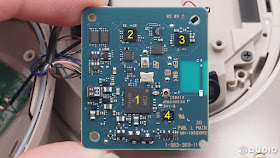
The Sony WH-1000XM4 has been unveiled by the FCC, the external photos do not provide anything new, they are the same ones as from the Anatel certification. The manual is the same but with English, the various details like battery, impedance and even power consumption are blank. The internal teardown provides even less detail but we do know the internal code finally, HDX-2943. I will go briefly over what we can see from these poor blurry photos but we will need to wait for a proper teardown to see all the details.
Update:
Looks like the WH-1000XM4 finally appeared on the Bluetooth certification site. Publish date says April 21st, but I do not recall seeing them there in that list, perhaps I missed it earlier. This BT certification finally confirms the Mediatek MT2811S Bluetooth chip, since the rest of this models in the list use this same chip. I know some people doubted me when I posted in the first FCC filing post back in December, that there was evidence pointing to a Mediatek chip.
The writing on the chips is impossible to read, so I can only compare the layout and various parts. So first comparing the side with the Bluetooth chip, the WH-1000XM3 looks like this:
Looks like the WH-1000XM4 finally appeared on the Bluetooth certification site. Publish date says April 21st, but I do not recall seeing them there in that list, perhaps I missed it earlier. This BT certification finally confirms the Mediatek MT2811S Bluetooth chip, since the rest of this models in the list use this same chip. I know some people doubted me when I posted in the first FCC filing post back in December, that there was evidence pointing to a Mediatek chip.
 |
| Click for larger size |
 |
| Image Source: 52Audio.com |
2. STM32L071CZT6 - Ultra-low-power ARM Cortex-M0+
3. Cirrus Logic CS47L15 - Low Power Audio DSP with smart codec
4. Q64FWY - 64mb serial flash memory
I did not mark the antenna here, but it can be seen on the right side in the box in the middle, the little silver rectangle.
Now comparing to the WH-1000XM4:
1. Bluetooth chip - from initial FCC filing, Mediatek chip, possibly MT2811S.
2. Ribbon cable connector - a new addition for this model, absent in WH-1000XM3.
A. Unknown chip 1
B. Unknown chip 2
C. Unknown chip 3
The unknown chips could be identical or similar to the ones from the WH-1000XM3, with the serial flash memory probably at 128MB now, like all new wireless headphones from Sony. A high resolution teardown from 52Audio will eventually come out and we will know what these chips are.
Now for the other side of the PCB.
 |
| Image Source: 52Audio.com |
1. QN1 - CXD90050
2. 100uF/6V Capacitors
3. Ribbon cable port 1
4. Ribbon cable port 2
5. Wires just soldered on
I am not sure where the wires in 5 go to but most likely to some controls or something, maybe someone knows where they go to by looking at the 52Audio teardown of the WH-1000XM3. If so, please post a comment below.
The WH-1000XM4 is similar but not identical.
1. Looks like the QN1 chip, unknown if different from current WH-1000XM3.
2. Capacitors, not sure if this says 107uf/6.3 or if it is still 100uF/6.3V. I did find a 100uF/6.3V capacitor in a Samsung document, CL43A107KQLNNN, so I suspect it is 100uF/6.3V.
3. Ribbon cable port 1 - identical to WH-1000XM3.
4. Ribbon cable port 2 - identical to WH-1000XM3.
5. Ribbon cable port 3 - Sony seems to have upgraded the soldered wires into one ribbon cable port, meaning these wires all probably went to one location.
6. Wireless antenna
There does appear to be another port like structure under the QN1 chip, but something similar was present on the WH-1000XM3 but there it was covered by see thru tape, so my guess is that perhaps it is a diagnostic or testing port. Moving the loose cables to a ribbon cable will help with repairs and packaging.
That is all I could gather from these FCC teardown photos, I am not an electrical engineer so I am sure I missed some major changes. If anyone sees such changes, please post below in the comments.


7 in 107 means 7 zeros so it's 100 000 000pF = 100uF
ReplyDeleteso are they basically the same thing?
Delete