The Sony NW-A300 internal documents have been available to download for a while but 2 of the files were not loading, so I decided to wait. Now all files are working, and we can finally get a good look at the inside of the new Walkman. The teardown is not a full one, but good enough to see what is inside.
Removing the rear panel will require the use of a heatgun or a heating plate to warm up the adhesive which holds the panel in place. The adhesive strips are shown with the red arrows.
There appears to be 2 clips/tabs (yellow arrows) which hold the top of the rear panel in. These will need to be un-hocked in order to free the cover from the main body. The cover appears to be made out of a plastic material, so it should be easier to remove than a glass back, but could still break as I am not sure if it is flexible or stiff plastic.
Removing the rear metal panel, reveals the battery and some of the connections to the PCB. The battery takes up the majority of the interior space.
The battery has 3 cables, red (positive), black (negative) and white (thermistor). The connections are soldered, so replacing the battery will be difficult for any soldering novices. In addition, the connections are very close together and near other components, so this adds to the difficulty level.
We can also see 2 ribbon cables, one for the side controls (long cable), and one for the 3.5mm audio jack, shorter cable.
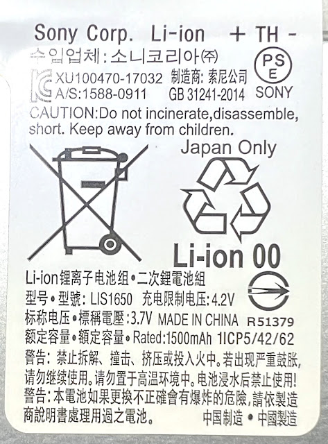
The battery model is the LIS1650, which can be found online if a replacement is required. I believe this is the exact same battery as in the Sony NW-ZX300. It has a 1500mAh capacity, which is more than the old NW-A100 battery, which was 1285mAh. This larger capacity is one reason why the new NW-A300 has superior battery life to the NW-A100. From the FCC documents, it appears that Murata is the manufacturer of the battery.
Removing the battery reveals the main PCB and the copper strip which we first saw in the comparison post.
 |
| Sony NW-A300 PCB |
Removing the PCB reveals the the another metal shield/piece which separates the LCD from the PCB. We can see the 2 cables/connectors I mentioned earlier, side buttons (1) and one for the LCD display (2).
Here is a clearer view of the PCB out of the Walkman. The wireless antenna can be seen at the bottom of the PCB.
Flipping the PCB over, shows the metal shields which are meant to cut out the noise from the components as not to interfere with the audio signal. The LCD connector near the bottom of the PCB (#1). The S-Master HX amp (CXD-3778) is visible in the lower left, along with the rest of the audio components. More on that later.
If we remove the metal shield, we can get a good look at the LCD display, well at least the back of it. Funny enough the person taking the photos for the documents seems to have used an iphone 13/14.
Here is a close up of the lower region (right) which is covered up by the smaller cover.
I am not 100% sure what this area is for, but I suspect it is related to the display, as a lot of the connections go to the display connector. If anyone knows anymore what the components are for, please leave a comment below.
Here is the close up of the audio processing section and the S-Master HX amp.
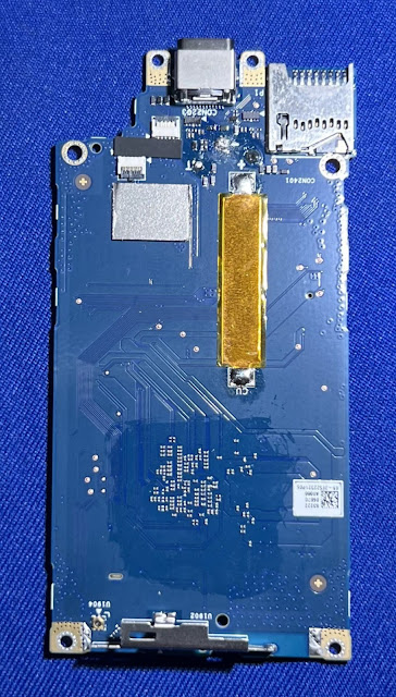
Here is a close up shot of the bottom portion of the PCB with the USB Type-C port, microSD card slot, the battery connections and the 2 connectors for the ribbon cables.
At the top of the PCB is the main wireless chip, which is situated near the wireless antenna, seen in the second photo. The main wireless chip is the Qualcomm WCN3950.
 |
| Sony NW-A300 Wireless Module - Qualcomm WCN3950 |
 |
| Sony NW-A300 wireless antenna |
The main chips under the central shield, are visible in this photo.
First we have the main SoC, the Qualcomm QCS2290. I have a write up of the SoC here.
 |
| Qualcomm QCS2290 - Main SoC |
Next up is the RAM, which is from Micron. It is a 32Gb, or 4GB chip. It is LPDDR4. The FBGA code on the chip is D8CJG, the part number is MT53E1G32D2FW-046 according to the Micron website.
 |
| Micron RAM |
Next is the main memory chip, 32GB from Samsung. The part number is KLMBG2JETD-B041.
 |
| Samsung flash memory |
Finally there is power supply module/chip from Qualcomm, the PM6125.
There is another chip under the cover, but I cannot make out what it is. If anyone knows what it is, leave a comment down below.
And with that this concludes the FCC teardown. The NW-ZX700 FCC filing also has some internal photos but not as many as the NW-A300. If I do make a NW-ZX700 teardown post, it will be rather brief.
I still have not bought a new A-Series, but even if I got one, I do not think I would take it apart.


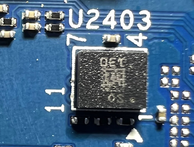
U2403 is a accelerometer chip.Manufactured by ST micro or Bosch.
ReplyDeleteexcellent cheers for that
Deletepower chip U4 is PM4125 rather than PM6125.
ReplyDeleteU2508 is the internal mono microphone according to the user guide
Do we know what the DAC is?
ReplyDeleteI don't think there is a dedicated chip, the S-master hx amp is what drives it.
DeleteGreetings, sir. What are the exact dimensions (width, height, and thickness) of the factory battery? of the Walkman NW‑A306? It’s for a friend.
ReplyDeleteThank you for your time and response.
I don't have that information. I can post photos of the battery beside a ruler from the fcc documents, but there is no thickness.
DeleteThanks you know if the battery lis 1623 the battery of the nw a100s is compatible?
DeleteShould be, but it has less capacity than the A300 battery.
DeleteI found one version of the 1623 with 2100 mah
DeleteHe encontrado esto en AliExpress:
30,18€ | Batería potente KiKiss de 2100mAh LIS1623HNPC para Sony Walkman NW-A35 NW-A45 NW-A46 NW-A47 NW-A55 NW-A56 NW-A57 NW-A105 NWA106
https://a.aliexpress.com/_EIQ7pwW
fyi, many products on aliexpress do not match the descriptions. So it may say, 2100mah, but it real world capacity will be less. Lots of dodgy sellers on there.
DeleteI understand thanks for the warning
Delete