Sony V1 Integrated Processor: A deeper look
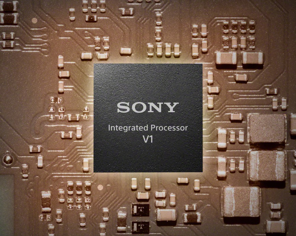
When Sony announced the WF-1000XM4 back in June, I was looking forward to seeing how Sony had improved the design and engineering in a teardown. In my main post, I did a quick teardown analysis of the device from the initial photos from Sony but this was not enough, but luckily a few days later the FCC report was finally available. The report labelled the Bluetooth IC and comparing it to Sony'press photos, it was clear the Mediatek MT2822 was the V1 chip. In that same post, I speculated that the V1 was a new chip integrating all the functions from the WF-1000M3, NC, flash memory and power management into one package. So was I close with my guess?
Now thanks to an EE Times article, we have a bit of information about the new MT2822 (V1). In their teardown of the WF-1000XM4, they used a report by Techanalye which used X-ray imaging to see into the chip. The first reveal is that we are looking at 2 layers, so a stacked chip.
 |
| Source: EE Times |
This photo shows the 2 different layers of the chip. According to the EE Times article, the top part is the analog layer and the lower part is the processing layer. The processing layer handles the AD/DA conversion and the analog layer is the power amplifier as seen in the last overview slide. In addition the processing layer also handles the Bluetooth 5.2 and noise-cancellation. (thanks aborne25 for the clarification).
 |
| Source: EE Times |
The article says that the chip incorporates 3 different function into one, with the analog chip being the amplifier portion. The Airoba AB1568 incorporates various power management functions, noise cancellation, Bluetooth and audio processing (see here), so perhaps the MT2822 is just a custom version of the chip for Sony. So even though there is no physical QN1e in the WF-1000XM4, the guts of the chip are present in the new MT2822. It would makes sense for Sony to want to combine 3 different chips into one package in order to save on space and power. Comparing sizes, the older MT2811 was 4.8 x 4.8 mm, while the AB1568 (MT2822) is 5.0 x 5.0 mm, so not much larger but incorporating a lot more tech.
 |
| Source: EE Times |
This final slide shows the various parts and how they are connected to the chip. The new Bluetooth section is much smaller and more compact now with the rest of the chip dedicated to noise cancellation and audio processing.The article also confirms that the chip was co-developed with Sony which could mean the MT2822 is just the AB1568 with Sony's own tech/algorithms integrated in, like DSEE extreme, QN1e NC algorithm, and so on (thanks aborne25).
One new piece of information from this photo is the 2 feed-forward mics for NC. Usually Sony uses one for feed-back and one for feed-forward, but it seems that both the voice mic and feed-forward mics can be used for NC. Perhaps the same scenario was present on the WF-1000XM3, but no idea how to test if that is the case. Unless the second microphone is used for wind noise suppression.
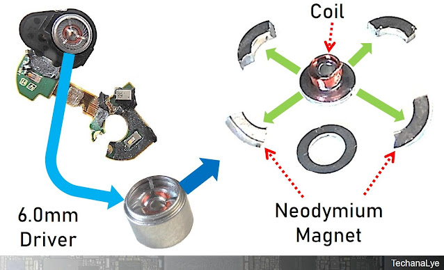
And a bonus photo, a teardown of the driver from the WF-1000XM4.
 |
| Source: EE Times |
If I had 2 WF-1000XM4's, I would definitely tear one down completely, but as it stands now, still saving up for my first one. The new WF-1000XM4 sport superior tech versus the older model, but this does not mean they do not have their issues as I am reading quite a few comments online about the foam tips not lasting very long for some users.
If anyone is able to find anymore interesting information from the article on EE Times, please leave a comment below.
Thanks to aborne25 from twitter for the article.


"If I had 2 WF-1000XM4's, I would definitely tear one down completely, but as it stands now, still saving up for my first one"
ReplyDeleteFunny reading this one. The whole has been serious until I laugh with this one
"I am reading quite a few comments online about the foam tips not lasting very long for some users"
ReplyDeleteI'd be more acceptant of this if the tips were actually available for purchase outside of Japan, because in my experience they're quite prone to cracking and nigh impossible to clean properly. (because unlike with silicon tips, you can't use water and a q-tip or paper towel)
and that's the problem, I feel Sony dropped the ball on this one. perhaps the tips offer better sound isolation versus other types but if they fall apart quickly, then what's the point. Sony only seems to offer the replacement tips in japan which is stupid. Offer the tips in all markets or don't offer them at all.
DeleteReplacement tips are actually also available for purchase in the US, though it's hidden in some Sony support page. There's a link to Encompass Parts at https://us.esupport.sony.com/support/s/model-accessories?language=en_US. If you search WF1000XM4 in the Encompass Parts page linked from the Sony support website, you'll find the replacement tips sold for $4.95 per tip(1 unit is 1 tip, not a pair, so a pair costs $9.9, and shipping's not included). I'm not sure where you can get them outside of the US or Japan, though.
DeleteSony should just offer the replacement tips globally, rather silly for them not to.
Deletereplacement tips, as well as ones that offer a better fit, are widely available. it's not a big deal. go buy a whole set of 10 replacements for like 15 bucks
DeleteI just got rid of them day 1 and to this day I'm using the regular silicone tips from some oppo buds laying around. NC works as good as with the original ones and last practically forever.
Delete