Sony V2 Integrated Processor: A deeper look
With the new WF-1000XM5, Sony has moved to a new processor, the V2, upgrading from the V1 in the WF-1000XM4. My question is why and how are the 2 processors different? I will try to answer these questions in my post.
Recall back to my Sony V1 post in 2021, where we found out that the V1 (Mediatek MT2822) was a 2 layer SoC which integrated the QN1e from the WF-1000XM3 into the Bluetooth SoC. In the original post we had some X-ray photos of the chips and while we might get something like that for the V2, it may be some time. On a side note, TechInsights has a teardown of the MT2822 in a report, but contacting them on Twitter yielded no replies, and since you need a corporate email to use the website contact, that option is out as well.
So I will stick with what facts I have gathered. From the Bluetooth certification, we have information which suggested that the V2 was the Mediatek MT2833. Well thanks to the FCC filing, we can confirm this finally. If that was not enough, an additional confirmation from a Mexican certification, also reveals the MT2833 as the main chip.
 | |||||||||||||
| Mexican Certification |
Introducing the GSBR-0002, the new SiP in the WF-1000XM5. Unfortunately we do not have any photos of the processor or the QN2e in this certification, it even says the SiP is sealed with resin and cannot be removed. While I doubt that, I will not be attempting to remove it if I buy a WF-1000XM5. I was hoping the FCC internal documents would reveal the chips, like with the LinkBuds S, but this is not the case. Here is a close up of the SiP and the back.
Scanning the Data Matrix code reveals this:
G2464S00EMERV4A00807G
No idea what this means, Googling the result yields nothing. If anyone has any ideas, drop them in the comments below. The GSBR-0002, looks like it has a version number, 4-3, similar to what we can see on the LinkBuds S' SiP.
 |
| Source: 52Audio.com |
The SiP is the GSBR-0001, with a version of 4-1. We already know what is under the resin, see this post, and what is interesting from the FCC filing, is that we have a version 2. This suggests that the chip has undergone several revisions. I have one more shot of the SiP which shows something else entirely.
This chip is from the manufacturer, more on that in a second, which has different text, ES2, which I am guessing would be Engineering Sample 2. I am not sure what the lower numbers represent.
So who is the manufacturer? That would be Goertek Microelectronics, or Goermicro. This SiP is on their website, but it is labelled as "TWS module". It is geared towards mid and high-range Smart Wireless headphones, and is described as:
Integrated bluetooth chip, DSP, power management chip, acoustic sensor and other functional units, can achieve wireless data transmission and audio call functions
These are the components/functions in the main Mediatek chip, with the rest possibly performed by the smaller chips surrounding it. I suspect Goermicro also manufactures the new GSRB-0002 module, but I have no proof yet. This photo is from a PDF on company's website.
 |
| Source: Goermicro |
We can see the LinkBuds S in the photo, along with the GSBR-0001. No company is listed, only JDM, which of course is Japanese domestic manufacturer, or Sony. It also mentions Gen2 TWS system SiP, which could very well be the GSBR-0002 in the WF-1000XM5, or something else.
So we now know for certain the V2 is the Mediatek MT2833. Naturally looking for any information about this chip yields very little, with most of the results from my own blog (hehe). From past and recent documentation, I have been able to ascertain that the MT2833 is either a custom or rebranded Airoha AB1588. Here is how I came to this conclusion.
There are no product pages for the AB1588, but we do have one for the AB1585. But are these the same chip? I was re-reading a discussion I had on reddit 2 years ago about the MT2811 and I finally realized what the person was referring to. I said that the MT2811 was the AB155X, but the user told me, that was odd since there are 6, yes 6, AB155x chipsets.
 |
| Source (link may not work anymore) |
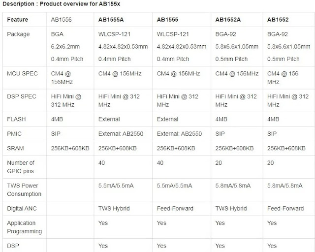
While not all 6 are present in this table, we have most of them. Recall this post from 2019 about the Mediatek MT2811. In that post, I calculated the size of the MT2811 to 4.8mm x 4.8mm. We have 2 chips in that table that match this size, the AB1555A and AB1555. The only different between these 2 chips is the noise cancellation, one is TWS hybrid and the other feed-forward. Likewise notice that both need external flash for memory, which is what we had in the WF-1000XM3 (Q128FWY). So I am guessing the MT2811 is just the AB1555A.
But what does this have to do with the MT2833? Well we can see Airoha has many chip lines and then different versions of each chip in that line. Let us look at the AB156X line.
 |
| Source |
An interesting revelation from this table is that the AB1568 is more efficient than the other 2 chips. While I have not seen any such tables for the AB158X line, we might only have 2 chips in the line up from what we can see on the Airoha website. The embedded flash can be either 8MB or 16MB, and from the 156X line, we can see that the AB1565 is 4MB and the AB1568 is 8MB. So I am going to go out on a limb and say the AB1588 is the 16MB version of the AB1585. This would mean the new V2 chip is a rebranded/custom version of the AB1588. The 16MB might be what Sony requires for their storage needs, as both the WF-1000XM3 and WF-1000XM4 used 16MB external flash chips.
With the chip now identified, let us take a look at its specifications and compare it to the V1 (AB1568).
| AB1588 (V2) | AB1568 (V1) | |
|---|---|---|
| Host Processor | ARM Cortex-M33F | ARM Cortex-M4 |
| DSP Processor | Cadence HiFi5 Audio Engine DSP co-processor |
Cadence HiFi Mini Audio Engine DSP co-processor |
| Bluetooth | BR EDR Bluetooth Low Energy LE audio Dual-mode |
BR EDR Bluetooth Low Energy Dual-mode |
| Power Management |
-Highly integration PMU -Li-ion battery charger for internal charging |
-Highly integration PMU -Li-ion battery charger for internal charging -Support BC 1.2 charger detection |
| Embedded Flash | 16 MB | 8 MB |
| Audio | Maximum sample rate is 192 KHz and data precision is 24-bit |
Maximum sample rate is 192 KHz and data precision is 24-bit |
| Hybrid Active Noise Cancellation(ANC) - Feedforward ANC - Feedback ANC |
Hybrid Active Noise Cancellation(ANC) - Feedforward ANC - Feedback ANC |
|
| Mono or stereo data transactions | Mono or stereo data transactions | |
| AI Noise suppression and echo cancellation |
Beamforming Noise suppression and echo cancellation |
|
| Multiband Programmable EQ and Dynamic Range Control |
Multiband Programmable EQ and Dynamic Range Control |
|
| Ambient sound | Ambient sound |
The chips are relatively similar, we do not have any power consumption figures for the AB1588, so unknown if it is more energy efficient. The host processors are also different. The AB1588 uses the ARM Cortex-M33F which has 20% more performance than the ARM Cortex-M4. The DSP processor is also newer on the V2, sporting the latest design.
Next major difference is the presence of LE Audio on the new chip, something absent in the V1. But we know the V1 (MT2822) supports LE Audio since the LinkBuds S support it and the WH-1000XM5 should also be receiving an update in the future. Finally the V2 has AI noise suppression, where as the V1 only has beamforming noise suppression.
I am uncertain if the AI functionality occurs in real time, perhaps it is only for calls?
So there we have it. The new V2 is either a rebranded or custom AB1588. There improvements over the original V1, like newer DSP and hot processor, but we still do not know if it is more energy efficient.
As for the question why did Sony switch to the new chip, well, I suspect Sony wanted the AI capabilities of the chip. Whether the new V2 also has the old QN1e integrated into it, is unknown, perhaps, Sony does call the chip an "integrated processor" like theV1. Another reason for the switch could be power consumption. While I have no evidence, I suspect the V2 is more energy efficient and might even be built on a newer process. Of course with Sony or Mediatek not revealing anything, we will never know anymore details

FCC Teardown
With the V2 chip identified, we can have a view at the FCC internal photos. With the exception of the GSBR-0002 SiP. the photos do not reveal anything else new. We do now have clearer and larger photos of the entire internal design, but no information about the battery or the chips under the SiP.
In this photo we can see that the flex PCB which connects to the main board is soldered to the antenna assembly. So if the antenna or touch sensor ever break, replacing them should be pretty simple once you get the earbuds open, and you can get your hands on spare parts.
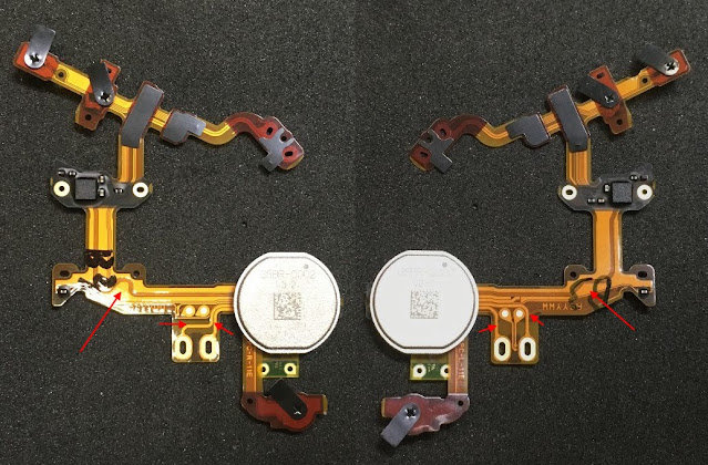
This second photo shows the entire flex PCB pretty well, much higher detail than before.
The GSBR-0002 looks to have a version of 3-2 written on it, so older than the 4-2 version earlier in the post. The small chip in the middle between is still not labelled and unknown. One thing I noticed is that there is a small difference in the design, which I have pointed out with arrows. The traces are a bit different from left to right, not sure why. Maybe it is for the manufacturing in order to be able to identify the sides? Anyone know why this is the case?
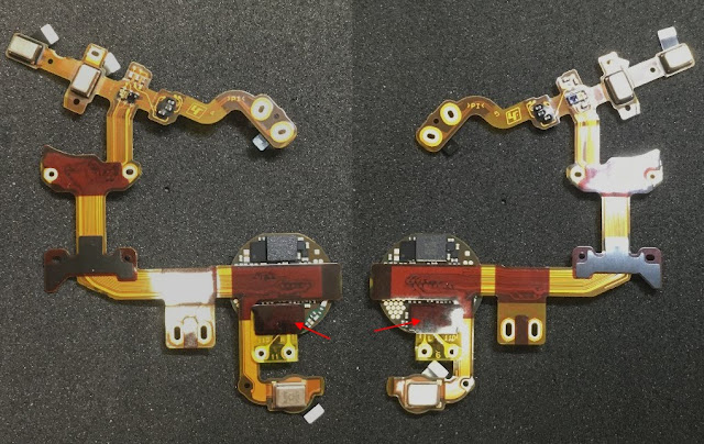
The next photo shows the reverse side.
Again, some minor differences in the layout of the traces, no idea why. The red arrow shows the small PCB which is connected via a board to board connector which then is soldered to the antenna/touch sensor assembly. For a description of the various parts, see my WF-1000XM5 post.
Here is one more shot from the FCC filing, showing the antenna, along with some measurements of the earbuds.
Well that concludes the teardown and the post. Maybe 52Audio will perform a teardown in the future, if not, I would love to do one but would have to save up money for 2 models, one to use and one for a teardown. There is little money Google Adsense and Amazon pull in, so it will be a while before I can buy anything,


Great posting. Many thanks for your work. It would be interesting to know whether the V2 makes use of an advanced chip manufacturing process and which one exactly is used.
ReplyDeleteThat was me :) E_D___B_A_N_G_E_R
ReplyDeletecheers. How are you finding the tips on the wf-1000xm5? seeing a few posts criticizing them.
DeleteI'm using the same size as on the XM4s and I have to say I don't find them that much different. The biggest difference is that the buds are now much lighter and that makes them much more comfortable, but the tips feel very similar. If you liked the old tips you'll also like the new ones and if you switched to third party tips one the XM4, you'll probably do it again.or over a year
DeleteI didn't and I won't do it on the XM5s. The only negative thing I can say is that I had to replace the ones that originally came with the XM4s at some point because they started literally falling apart, but the ones I bought as replacement (Sony EP-NI1000) lasted without a problem until I received the XM5s
E_D___B_A_N_G_E_R
Great work! Very good research. Wish Sony would be more informative with the hardware changes.
ReplyDeleteNew Sony Playstation headset & earbuds officially announced.
ReplyDelete"Pulse Elite and Pulse Explore connect directly with PlayStation Portal by leveraging this new wireless audio technology, PlayStation Link. This innovation delivers low latency, lossless audio and easy switching between multiple PlayStation Link hosts such as PS5 with the USB adapter and PlayStation Portal."
https://blog.playstation.com/2023/08/23/playstations-first-remote-play-dedicated-device-playstation-portal-remote-player-to-launch-later-this-year-at-199-99/
Looks like PS Link is based on WiFi instead of Bluetooth. Battery runtimes would be interesting and of course also whether this will be implemented in other devices like Xperia smartphones and of course Walkmans in the future.
E_D___B_A_N_G_E_R
It looks like it is the new chip, CXD3277GG, mentioned it here in an update a while ago.
Deletehttps://thewalkmanblog.blogspot.com/2023/07/sony-yy2977-yy2980-appear-on-bluetooth-sig-are-these-the-playstation-earbuds.html
Eres increíble amigo, que buen aporte, disculpa que hable en español, pero quería darte las gracias por tan buen aporte e investigación, bastante interesante todo, muchos éxitos!!
ReplyDeleteSo is the DAC also integrated into this SoC?
ReplyDelete